
This tutorial is for use with the Altera DE-nano boards. There are a number in the eshop. See Mary if you cannot find one.
In this tutorial, we will program the DE-nano board, to be a simple 3 bit counter. The leds labelled led1, led2 and led3 will be the outputs. The values will change each time Button1 is pushed. Button4 works as a reset button.
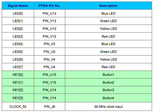
Here are the pin assignments for this board.
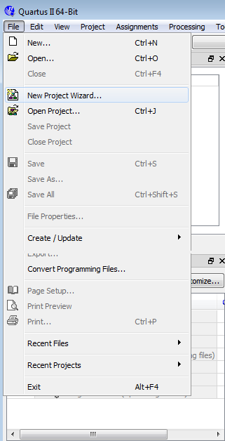
After starting Quartus, do File -> New Project Wizard
Click Next
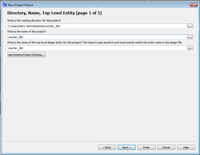
Give your project a name and directory. Hint, don't start the name with a number.
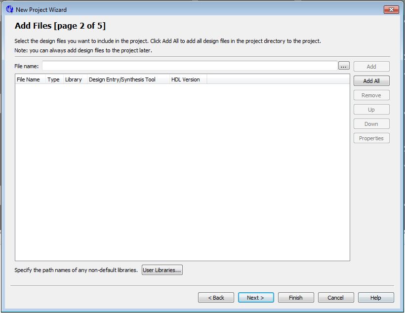
Click Next on the Add Files page
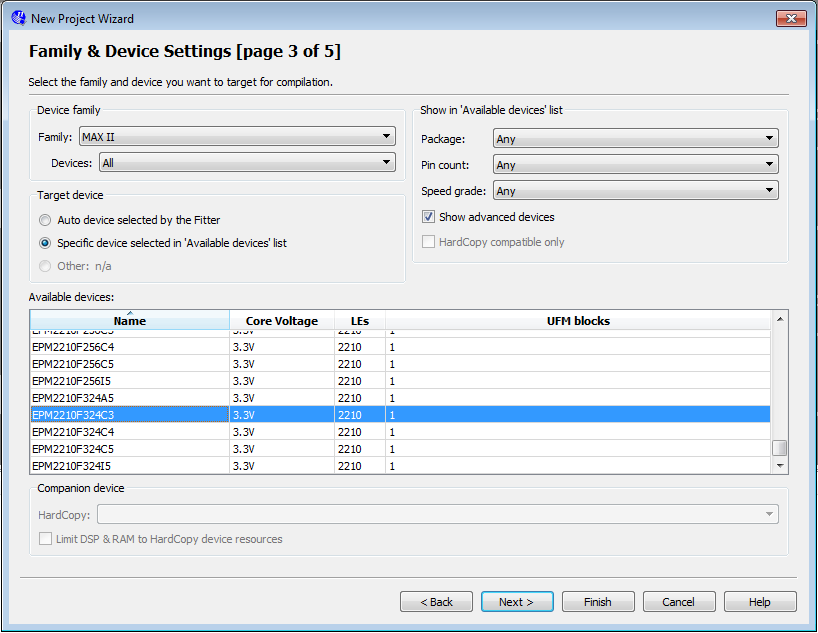
Choose the device on our board. Family: Max II, Device: EPM2210F324C3 and click FINISH.
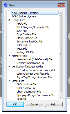
File -> New and choose "Block Diagram/Schematic File" from the window that comes up.
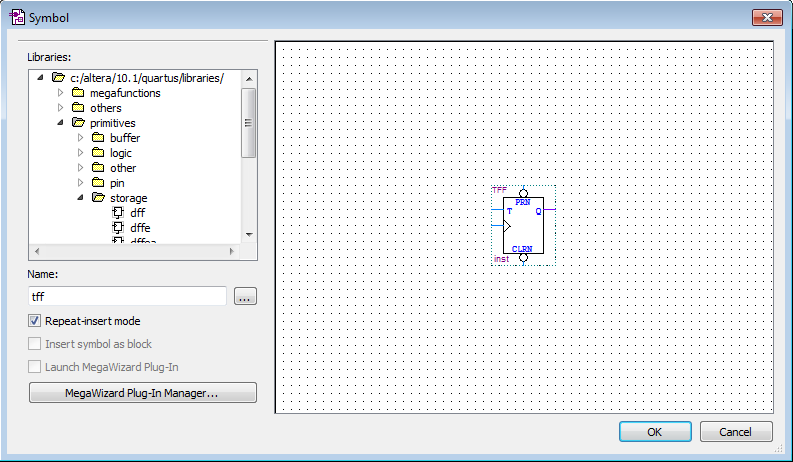
We need to place parts in our block diagram. Click the Symbol Tool (located next to the A in the top bar of the block diagram) to bring up the symbol window. Find the tff, you'll want to place three in your block diagram.
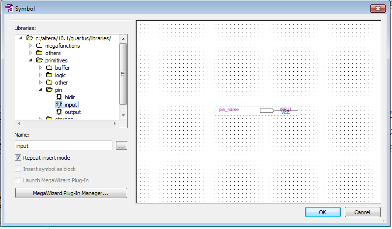
Repeat, but this time place two input pins.
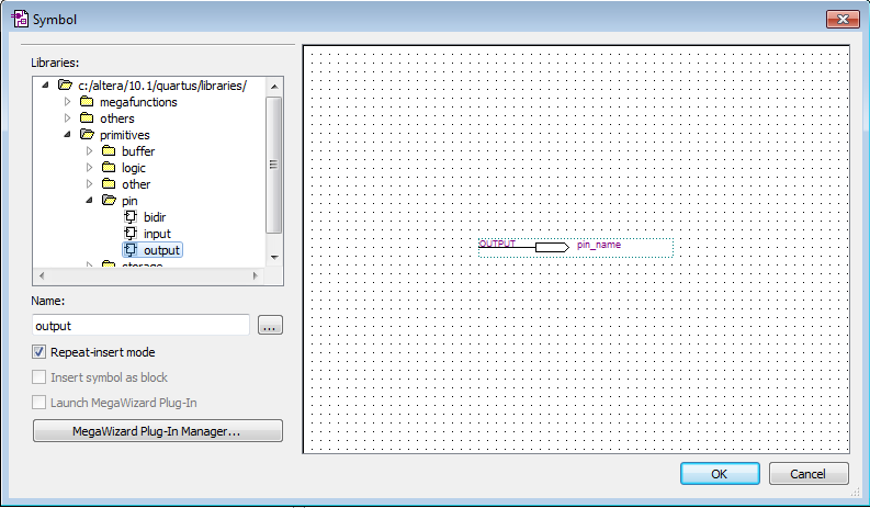
Now place three output pins
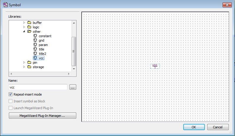
Lastly, place a vcc
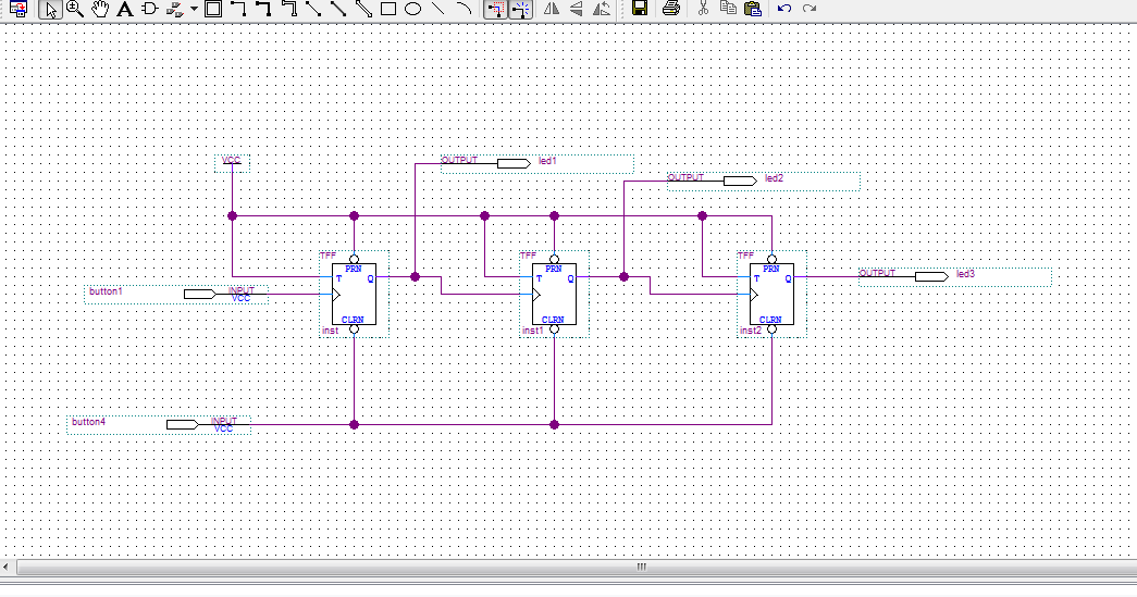
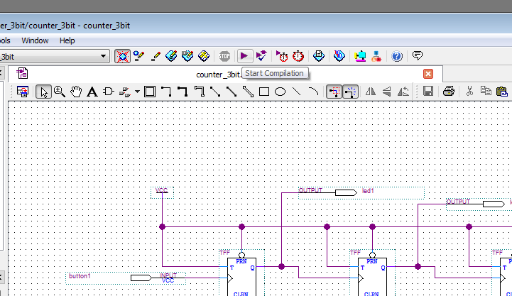
The block diagram should now look something like this.

Use the 'Orthogonal Node Tool' to connect the parts so that your block diagram looks the same as the one below.
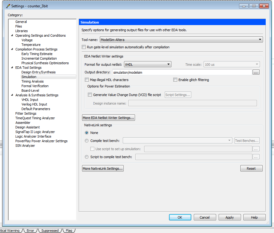
Later, we are going to use Modelsim to simulate our project. So we need to tell Quartus to generate the files needed by Modelsim. Go to Assignments -> Settings and select Modelsim-Altera in the Tool name field. Do not check the "Run gate-level simulation automatically after compilation" box.
Compile the project (click the purple triangle).
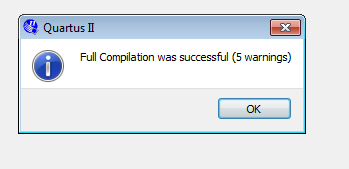
If you get errors, read through them to try to figure out the problem. Successful compilation will give this window.
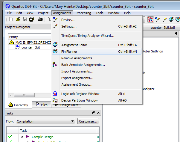
Now we need to assign pins. Start the pin planner.
Double-click in the location to either select or type in the pins.
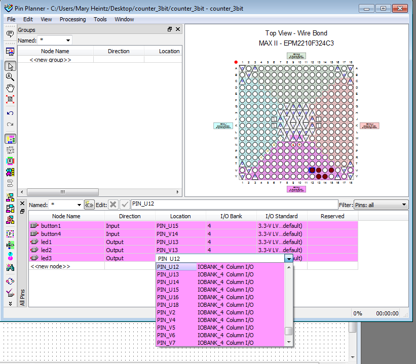
After assigning pins, recompile the project!
We will use Modelsim-Altera to perform a functional simulation.
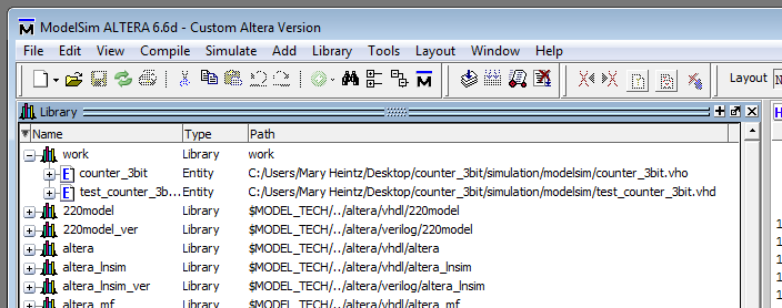
Start Modelsim and do File -> Change Directory
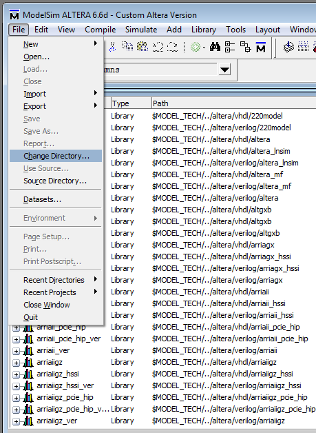
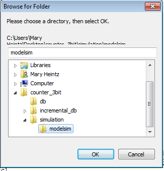
Select the simulation/modelsim directory that is inside your project directory.
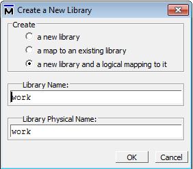
File -> New -> Library
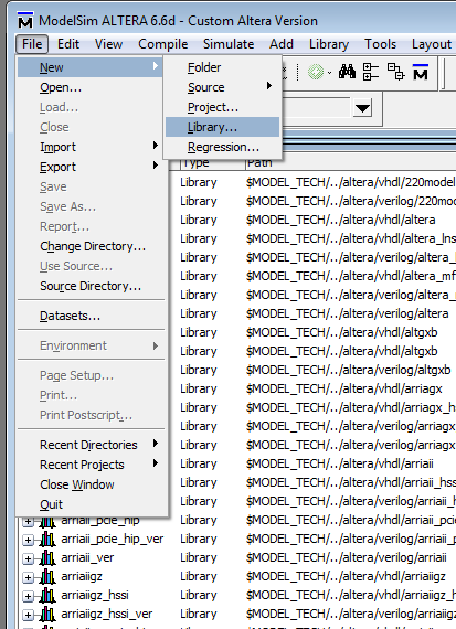
Make a new library. Work is the default name and is fine.
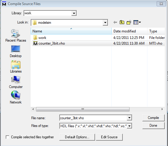
Compile the counter_3bit.vho file. It will be in the work library when finished.
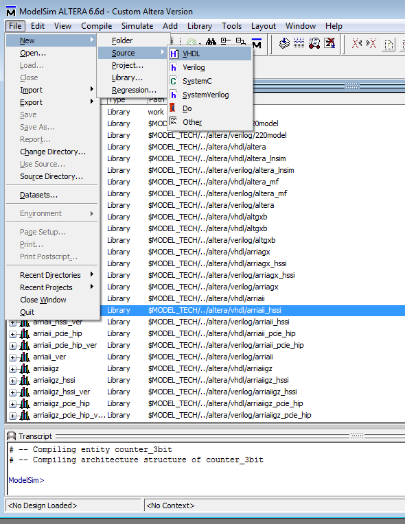
We need to create a testbench to use to simulate the project. This testbench is just a VHDL file. So create a new one, File -> New -> Source -> VHDL
Here is the text for a very simple testbench.
-- testbench for counter_3bit

-- Load Altera libraries for this chip
LIBRARY IEEE;
LIBRARY MAXII;
USE IEEE.STD_LOGIC_1164.ALL;
USE MAXII.MAXII_COMPONENTS.ALL;

-- Set up this testbench as an entity
entity test_counter_3bit is
end test_counter_3bit;

-- Create an implementation of the entity
-- (May have several per entity)
architecture testbench1 of test_counter_3bit is

  -- Set up the signals on the 3bit_counter
  signal button1 : std_logic;
  signal button4 : std_logic;
  signal led1    : std_logic;
  signal led2    : std_logic;
  signal led3    : std_logic;

  -- Set up the vcc signal as 1
  signal vcc  : std_logic := '1';

  begin
    -- dut = device under test (same name as top project from Quartus)
    dut : entity work.counter_3bit
      -- Map the ports from the dut to this testbench
      port map (
        button1 => button1,
        button4 => button4,
        led1 => led1,
        led2 => led2,
        led3 => led3 );

    -- Set up the signals
    stimulus : process is
      begin
        -- Just make a clock on button1 to simulate pushing the button
        loop
          button1 <= '0'; wait for 10 ns;
          button1 <= '1'; wait for 10 ns;
        end loop;
      end process stimulus;
end architecture testbench1;
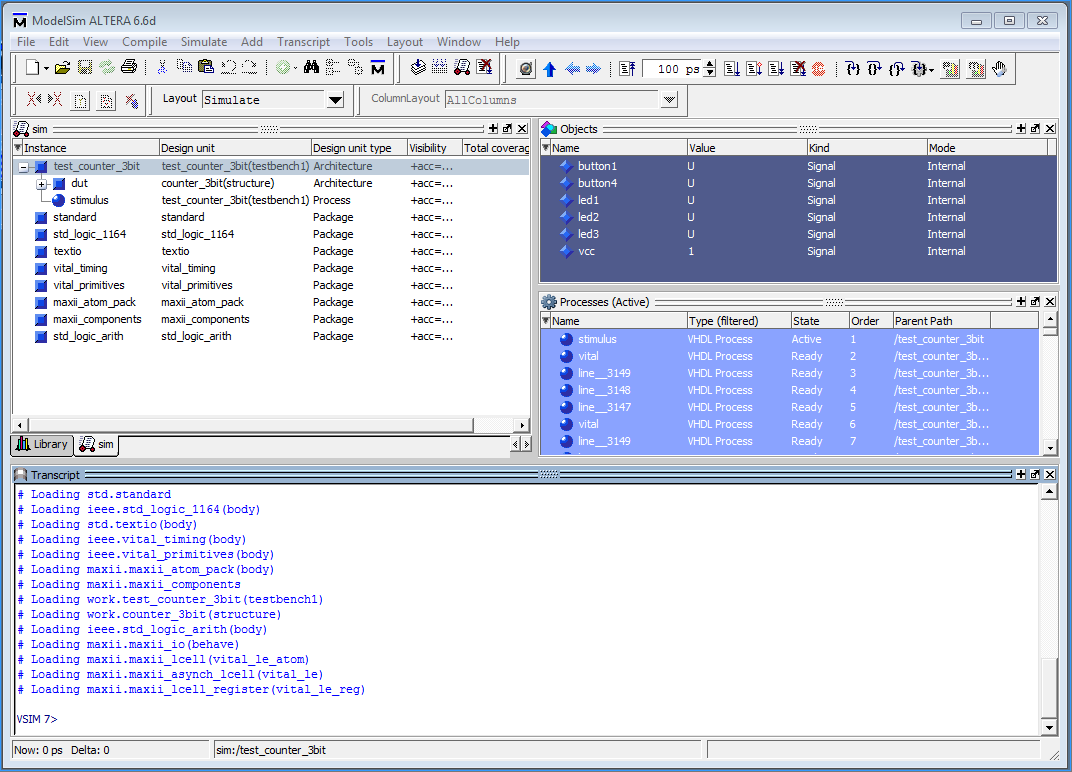
Now, we must compile this testbench into our work library. Same as before, pick Compile and select this file, here saved as test_counter_3bit.vhd.
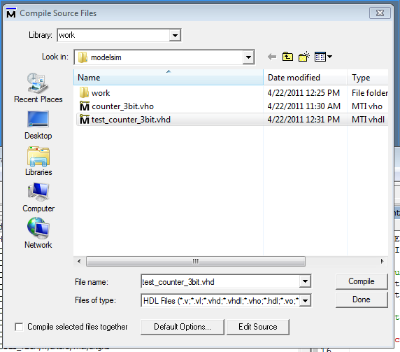
Now our work library should have two files in it.
Double-click on the testbench (test_counter_3bit) to start simulating. A number of windows will open. You can close the testbench text editor. The window should look something like this.
Open the wave window. View -> Wave
Then drag all the objects (button1, button4, led1, etc.) in the Objects window to the Wave window so that they will be plotted.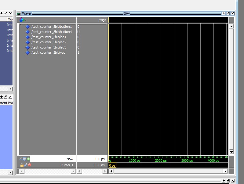
Click the Run Simulation button to run the simulation for 100ps. This is going to be much too short, so change the length to 10000 ps and click run. You'll then have to play around with the zoom on the window to get it so that you can see the clock and the results.
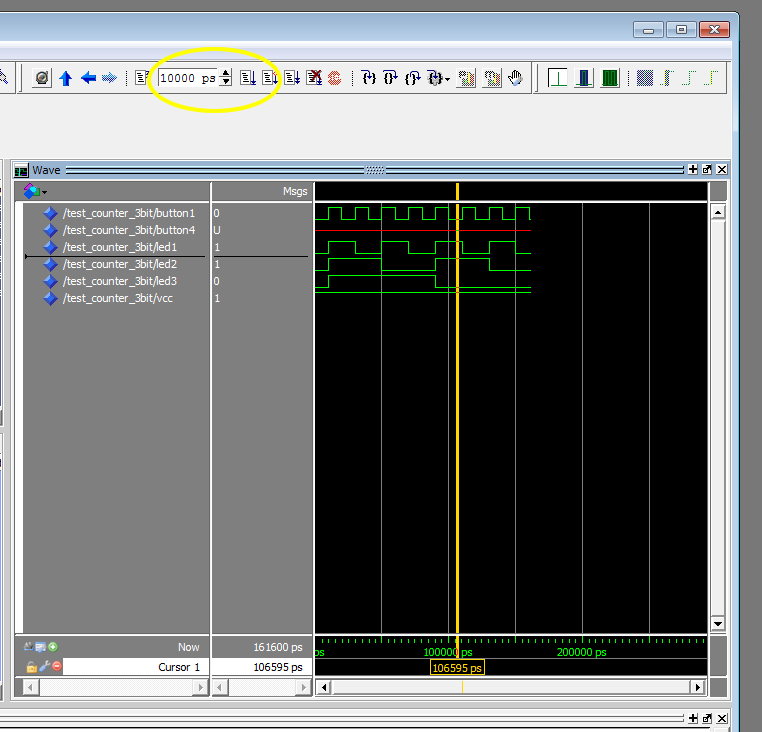
You'll have to look very closely at your output to see that things are actually working as expected. You also should do much, much more simulating that what is here. This is just to show you how things actually work. At this point, I'm assuming that everything works as expected and we now want to program our chip. Quit Modelsim.
Back in Quartus, we will program the chip. Before plugging the DEnano board in, check the settings on the jumpers circled below. One needs to be up and two needs to be down to be able to program the chip.

Open the programmer, Tools -> Programmer.

If the USB-Blaster[USB-0] is not showing in the Hardware Setup, click on that button and select it. If you cannot find it, let Mary know so that the driver can be installed in Windows.

Check the boxes under Program/Configure and then click the Start button.

While programming, all lights except the blue power and load buttons should go off. It will take a minute or two for the program to upload. When it's finished, try clicking button1 and button4 and see if things work as expected.