Status
March 23, 2006 - More noise tests.
Reinstalled two LDOs: U565 and U576.
(These parts were replaced in the summer with ferrite beads to reduce
the total power consumption. At that time, only rms noise levels were tested
and this change didn't seem to affect performance.)
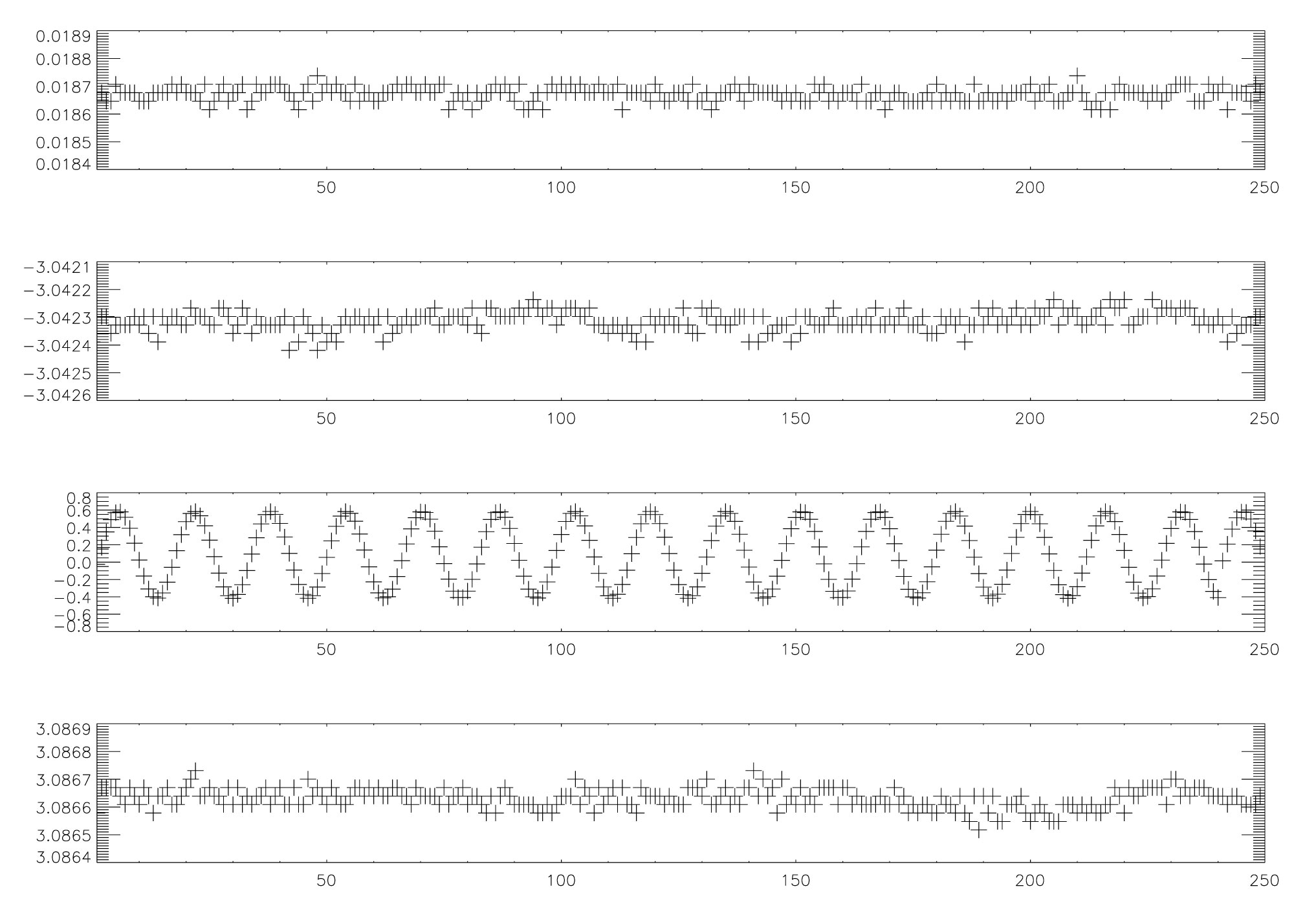
With the LDOs installed, the noise spikes recorded were greatly reduced
on both boards.
The plots with the recorded noise data with the LDOs installed are
here: card1_r.pdf, card2_r.pdf.
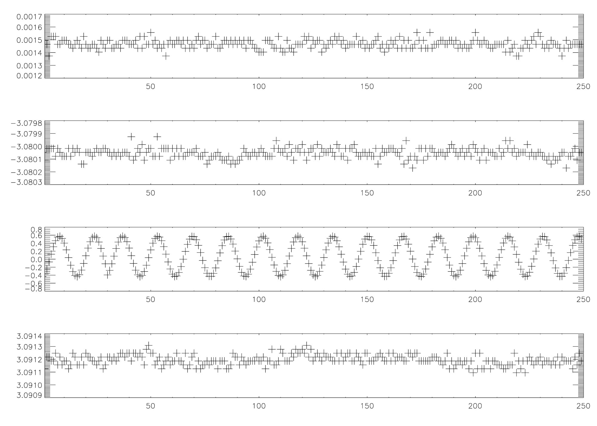
Repeated these tests with fuses F5Van and F7Van replaced with ferrite
beads.
The plots with the recorded noise data with the LDOs installed and
ferrite beads instead of F5Van and F7Van are here: card1_br.pdf,
card2_br.pdf.
Observation:
Since the heatsinks installed on U565 and U576 are very small, we reduced
the crate 12V power supply level to 8V. If the board is to be used in a
crate with an actual 12V supply, the heatsinks would have to be replaced
with larger ones.
March 20, 2006 - Noise tests.
Test data acquired, with nothing connected at the board inputs showed
some FFT spikes at 100Hz and 4kHz.
All data are read out via the VME backplane at 10 ms time intervals;
that's where this noise seems to come from.
In order to test correlation between the input filters and the spikes,
changed the boards as follows:
Board 1 has:
Aj_20, Aj_25=15 Ohm for j={0,...,3}U{8,...,23}U{28,...,31} - rows:
1,3,4,5,6,8.
Aj_20, Aj_25=100 Ohm for j={4,...,7}U{24,...,27} - rows: 2,7.
Board 2 is vice versa.
Note that fc=590kHz for 100 Ohm and fc=3.9MHz for 15 Ohm (C=2.7nF on
both boards).
Also, the digital acquisition timing changes slightly with the resistor
values.
Found clear correlation between the recorded 4kHz noise and the input
filter, but not with the 100Hz noise.
The channels with the 100 Ohm resistors showed the 4kHz noise. It could
actually be some issue with the acquisition timing...
The plots with the recorded noise data are here: card1_b.pdf,
card2_b.pdf.
Also, by doing this test, found a small FPGA firmware bug: the channels
in row 6 and 7 were switched.
Feb. 2006 -
Board 1 has: Aj_19,Aj_27 = 1.2K; Aj_17, Aj_28 = 2.4K; Aj_20, Aj_25=15
Ohm.
Board 2 has: Aj_19,Aj_27 = 1.2K; Aj_17, Aj_28 = 2.4K; Aj_20, Aj_25=100
Ohm.
Oct. 31, 2005 - Some more temperature tests.
May 9, 2005 - Testing of the partially stuffed board is finished and the kit with the parts for manufacturing of two Q_ADC boards is out.
April 20, 2005 - Fixed some minor bugs in the FPGA design and recorded
A to D converted data via VME.
The Q_ADC board seems to work as specified.
The 4 channels have: -3Vdc, 0V, +1Vpp sine and +3Vdc at the inputs.
We used the old and noisy 9U VME crate in the shop.
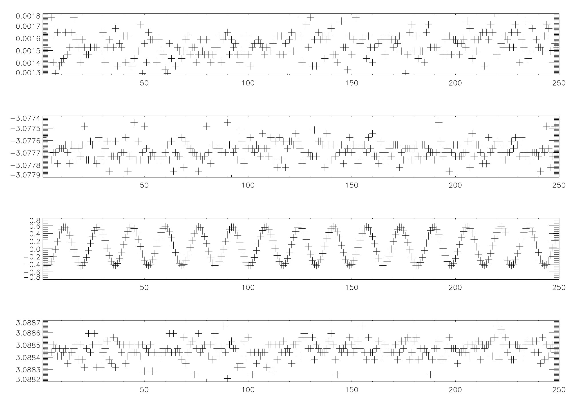
The board has one-pole low-pass RC filters for the analog signals that may or may not be soldered (the cutoff frequency can be changed also).
Here are plots of recorded data without
the filter installed and of the recorded
data with R=15Ohm,C=2.7nF (fc=3.6MHz)
and of the recorded data with R=100
Ohm, C=2.7nF.
Note that the noise level can be further reduced by reducing fc. Since
the sampling rate is 800kHz, we can go down by a factor of 10 and reduce
the noise even more; have to see what effect this has over the transition
spikes on the 4 kHz signal.
So far, the old switching power supply seems to be good enough.
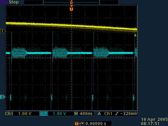
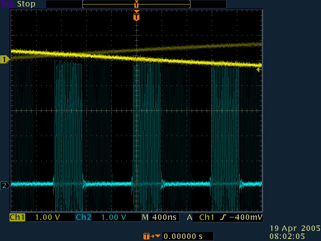
April 19, 2005 - Installed first draft FPGA design with 4 channels of
raw data recording and scoped some lines;
- the _CNVST pulses (800
kHz);
- the acquisition clock
(bursts of 25 ns pulses every 1.25 us).
Recorded some data (1000 words) via VME block transfers. Have to make
some sense out of it.
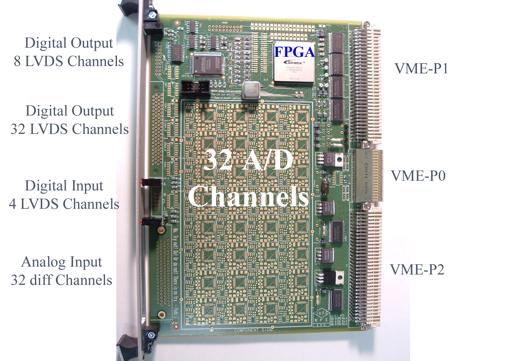
April 14, 2005 - Finished partial component soldering in the shop (no
ADC channels yet). See picture of partially
stuffed board.
Loaded design (U:\designs\QADC\sigma_delta\sigma_delta.quartus) in
the FPGA and performed VME transactions as presented in this transcript.
The board seems to work as specified; it is alive and one can talk
to it.
Note that the loaded design includes the VME and CSR blocks only, not
the ADC control part.
A more complete design revision will have to be loaded to test the
ADC part of the board.
Problems found and solved:
- two bad solder joints on the board;
- the 9U/6U VME extender card has no passing of GA[4..0], which is
actually O.K. when used for the crate CPU; fixed that.
To do:
- install a few ADC channels, we should do that tomorrow;
- get a new FPGA design revision ready to test the ADC channels;
April 13, 2005 - Received 1 piece bare PCB with one FPGA installed. Started soldering in the shop of the rest of the components except for the ADC channels.
April 8, 2005 - Sent 1 piece bare PCB and 1 piece FPGA (BGA) to the assembly house for installation.
April 7, 2005 - Received bare PCBs from manufacturer.
March 22, 2005 - Performed full schematic digital simulation of VME
transfers with three QADC boards in a VME crate, using QuickSimII by Mentor
Graphics.
Here is a plot of some successive VME
write commands on a board in slot 7, followed by some VME
read commands from the same board.
March 21, 2005 - The gerber files are out.
March 18, 2005 - Performed some signal integrity tests on the QADC board.
March 16, 2005 - Schematic capture is 100% done, same with board design
and layout.
The VME part of the Altera FPGA design is finished and simulated with
QuartusII.
QuartusII Simulation plot of some VME writes can be found here: writing
of control registers.pdf
Feb 11, 2005 - Schematic capture for the ADC board is 50% done, same
with the board design and layout.
FPGA design has started.