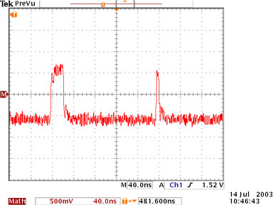
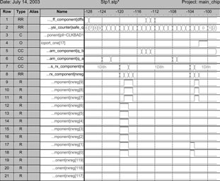
These two plots present LVDS pulses through a 1ft cable, recorded with scope and with Signal Tap inside the Stratix device:
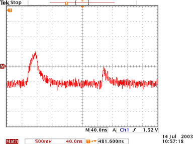
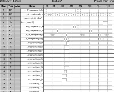
Same here, but in this case we have a 47pF cap on the line:
(the short pulse is to small to be recorded by the LVDS receivers)
Jan-Feb. 2003:
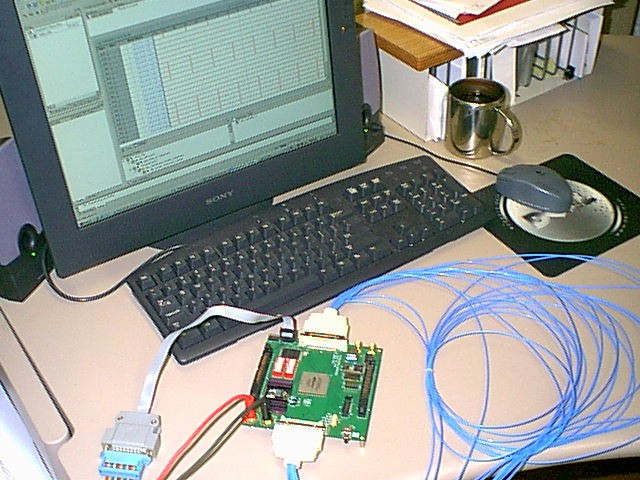
Using an Altera FPGA Development Board Q5V1
by Rowe Engineering, we implemented in the same chip a 12 channel LVDS
pulse
generator and we fed the signals back into the chip's SERDES
Time to Digital Converter (see below picture).
We used cables of different lengths (6" increments), to create delays
so different inputs received pulses at different time intervals.
The output of converter was read with ByteBlasterMV
using SignalTap.
This page was last updated
by Mircea Bogdan on August 28, 2003