Using our Altera FPGA Development Board Q5V1
by Rowe Engineering, we implemented a 12 channel LVDS Test Pulse Generator
(TPG) with the following pattern:
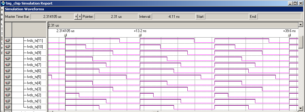
Here's a simulation of the outputs
for Wire11..0, as seen in QuartusII.
This pattern is not in phase with the CDF Clock but it repeats itself
in a continuous flow.
Test procedure:
Plugged TPG to the TDC Board FP2. (Wire_0 -> TDC_Channel_35, Wire_1
-> TDC_Channel_34,...,Wire_11 -> TDC_Channel_24)
Plugged connectors with the negative inputs shortened to GND to FP1,
Fp3, FP4. (TDC_Channel_95,...36,23,...0 = High.)
Generated one L1A pulse with the Test-Clock Board and one L2A pulse
via VME.
Compared the TDC-measured pulse widths and time intervals between pulses
with the TPG pattern.
Repeated the L1A/L2A succesion 12 times.
This transcript presents the VME comands
as well as the Hit Count and Hit Data info from the board's VME readout
buffer.
Results:
From these tests, we conclude that the minimum pulse width is
4.8ns (4 bits) +/- 0.6ns (1/2 bit)
and the double pulse resolution (minimum interval between pulses) is
also 4.8ns (4 bits) +/- 0.6ns (1/2 bit).
Observation:
As expected, some half the time in this test setup, the TDC receiver
drops a bit from a pulse. Some times it picks a bit.
We learned from previous experiments with our TPG that a 4-bit (4.8ns)
generated pulse may be seen as a 3-bit pulse by the TDC receiver and not
be recorded as a hit at all.