Status
Dec.15, 2004 - Full crate CBLT tests at Fermilab.
Used the same simple vme readout programs as in previous CBLT tests.
Started with 2 boards and moved up to 16 boards in the chain. CBLT32
works well over the whole crate for both Hit-Data and Hit-Count buffers.
Measured the speed by scoping
the *AS line on the backplane and got 15.75 MBytes/s for one 3,328
Bytes CBLT32 transfer, over 16 boards in the crate.
I think the speed could be increased by reconfiguring or changing the
crate CPU.
Obs: there is an error on CBLT64 Hit-Data Buffer readouts with more
than 260 words. The software reads one VME word less than specified.
I think this is an easy to fix software error. CBLT64 works well over
the whole crate for Hit-Count Buffers readouts (128 64-bit words).
Oct.1, 2004 - More tests on board 4 in slot 10, using our Test Pattern
Generator.
Generated L1A with the TestClock and L2A via VME and examined the hit-count
and hit-data info from the VME read-out buffers.
The "edge-detected" pulse widths and time intervals between pulses
seem to be fine. See transcript
(uncommented).
Sept. 25, 2004 - Just finished the new CBLT64 VME firmware and just
tested it with
two preproduction TDC boards in our crate. Firmware and boards
work as designed.
I can do both CBLT32 and CBLT64 transfers on both Hit-Count and Hit-Data
Buffers.
Transition is automatic.
Measured the speed by scoping the *AS line on the backplane
and I got 18 MBytes/s for CBLT32 and 35 MBytes/s for CBLT64
For some scope-plots, look in here: http://edg.uchicago.edu/~bogdan/tdc/CBLT_tests.html
For transcripts of what I tested today, look in here:
http://edg.uchicago.edu/~bogdan/tdc/scope_plots/CBLT_32_64_transcript.txt
So far, so good.
July 8, 2004 - More Tests, using the Altera Stratix Development Board 5QV1.
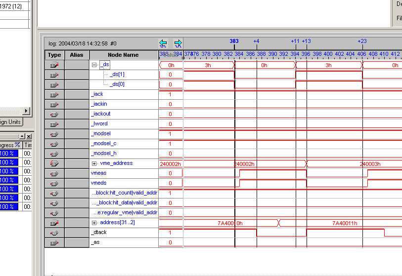
March 18, 2004 - Performed CBLT for the hit-count buffers only, using
two TDC boards, in slots 14 and 15.
It seems to work fine. The second board has no Stratix chips installed,
so it only reads FFFFFFFF.
Repeated the transfer with the boards switched.
Will do more tests, including reading of the hit-data buffers, whed
the other two boards come in.
Changed DLc and DLh to DDU7C-100 to increase speed and changed 1 line
in the VME chip code to accomodate.
The transcript for reading 28 words over two boards can be seen here.
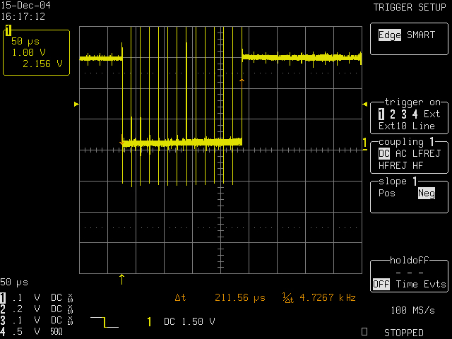
For a reading of 20 words over two boards, measured AS* low for 4.726us.
For timing info, here
is the screen shot of SignalTap, with 10ns sampling rate, inside the VME
chip on the
second board during an actual CBLT. Our crate computer seem slow.
Note that I had to "fix" a little
the active daisy-chain jumpering in our backplane to make it work...
March 16, 2004 - Tested CDF Clock Delay Blocks by writing different
values on Addr YY000020 and YY010020
and observing the delayed clocks with the scope. Bd #2 works fine.
On Bd #1 only one delay block works.
I think the Programmable Delay Line is defective. (We'll order some
and replace it.) Having a second board for
comparation, was very handy and saved me a lot of time.
Created a test design to generate pulses for the XFT output to P3.
It is a 16 bit counter for Data(15:0), the 22ns strobe is just passed
through, and W0,B0 are_strobe.
Loaded Bd#1 with the test design and scooped the P3 footprint on the
PCB (P3 is not installed yet on any board)
according to Specification for XFT Frontend,V1.0, March4th, 2003,(blw).
The pulses look OK.
March 15, 2004 - Changed the firmware and included SignalTap.
First compilation attempt with a sample depth of 512 did not fit. Changed
it to 256.
Implemented a test pattern generator (TPG) with our little development
board,
that can be plugged in any of the 4 front panel connectors of the TDC.
It generates a pattern of 3
standard LVDS pulses on 12 wire pairs.
The pulse widths are: 6ns, 6ns, 12ns and starting times: 0ns, 24ns,
90ns.
The pattern is the same on
each wire pair and repeats every 396ns, not in phase with the CDF clock
(but it can be).
For the other 12 input pairs on the connector, the negative input is
connected to GND to avoid crosstalk.
Note that Vcom for the LVDS termination on board is set to 1.4V as
for the pseudo LVDS pulse generator.
Performed the following tests on TDC board #2:
-Using SignalTap with JTAG, we looked at the output of the pipe with
the TPG plugged successively
in each of the four FP connectors. It looks fine.
-We plugged the TPG to Conn1.
Generated L1A with the TestClock and L2A via VME and examined
the hit-count and hit-data
info from the VME read-out buffers.
The "edge-detected" pulse widths and time intervals between pulses
seem to be fine.
Still to check (hardware):
- connection and functionality of CDF_B0, CDF_BC, CDF_L2A,
- connection and functionality of CDF_CLK delay block
- connections and functionality of the XFT block
- connection(*IACKIN/*IACKOUT) and functionality of CBLT block
March 11, 2004 - Mary debugged the Edge-detector block, reconfigured
the chips on board #2 and generated many Level 2 Accept
pulses via VME for various L2 Buffers. The results
seem to be OK. We will put the new programming files in the configuration
devices.
March 9, 2004 - The first two assembled boards are in. So far, the hardware
seems to work fine; I did VME writes and reads
to/from most memory locations. Also, I implemented the L2 Accept via
VME and I put different Memory Initialization Files
in each of the four L2 buffers. So, at power-up we have the L2 buffers
loaded with known data and a set of successive L2 Accepts
via VME can act as a rudimentary and partial self-test.
After fixing some firmware bugs in the edge detector block we should
be able to input some pulses to the board, using our little
test-board as a generator.
Jan. 2004 - The Gerber files are out.
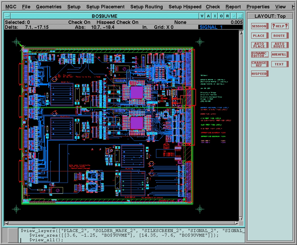
Jan. 2004 - TDC board Layout - Screenshot.
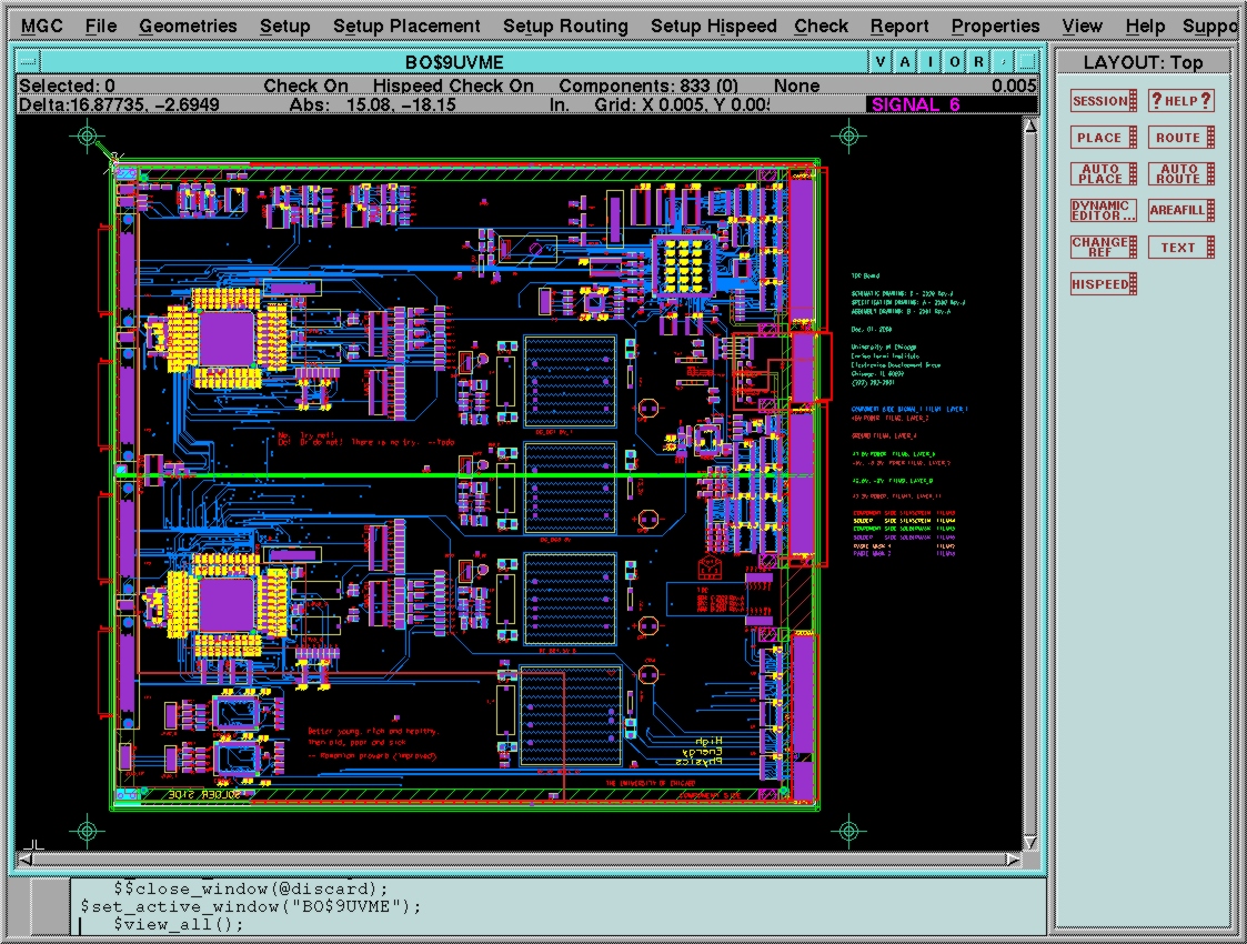
Dec. 2003 - TDC board Old Layout - Screenshot.
Sept. 2003 - Schematic capture for the TDC board is 50% done, same with
the board design and layout.
Main chip still has bugs that need fixing.
July 2003 - XFT Block design changes, following the TDC review meeting.
July 2003 - More Tests with the Altera Development Board Q5V1; we included slow rising pulses.
June 2003 - Design work for the main chip is basically finished,
some minor bugs need still to be fixed and pins need to be assigned.
Same with the VME Interface chip. Schematic capture for the TDC board
has started.
April 2003 - Design work for the new VME Interface chip with Chain Block Transfer capabilities has started.
Feb. 2003 - Tests with the Altera Development Board Q5V1; time delays are measured and recorded using Signal Tap.
Dec. 2002 - Design work for the two identical Stratix devices
on the board started.